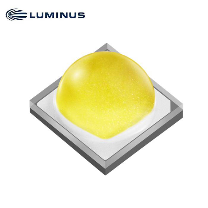
Description
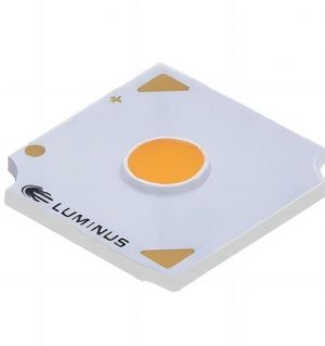
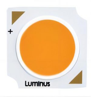
SST-36F-W-AL The F-Line High Power White LEDs
Features
• The flip chip in an optimized ceramic package has a typical light output of 741 lm @ 1.5 A, 85 °C (6500K).
• Excellent cost per lumen performance.
• Luminous Efficacy: Up to 176 lm/W @700 mA, 85°C (6500K)
• Maximum Drive Current: 3 A
• Color Temperature: 5000K, 5700K, 6500K
• Color Rendering Index: 65, 70
• Low thermal resistance: 1.9 °C/W
• Standard ANSI-compatible central 4 chromaticity bins.
• Electrically isolated thermal path.
• 8 kV HBM ESD rating per ANSI/ESDA/JEDEC JS-001.
Applications
• Outdoor and Roadway Lighting
• Indoor and Linear Lighting
• Stadium Lights
• Flood Lights
• Work Lights
• Portable Lights
Ordering Part Numbers
| CRI | CCT | Luminous Flux | Chromaticity
Bin Kit3 |
Ordering Part Number | |
| Minimum Flux Bin1 | Minimum Flux2 | ||||
| Min. 70 | 5000 K | G1 | 680 lm | 502 | SST-36F-WE50-AL-G1502 |
| 5700 K | G1 | 680 lm | 572 | SST-36F-WE57-AL-G1572 | |
| Typ. 70
Min. 65 |
6500 K | G1 | 680 lm | 652 | SST-36F-WS65-AL-G1652 |
| G1 | 680 lm | 705 | SST-36F-WS65-AL-G1705 | ||
Luminous Flux Bins
| Flux Bin | Binning @ 1500 mA | Correlated Minimum Flux (lm) @ Tj=85°C2 | ||||
| T = 85°C1
j |
T = 25°C
j |
|||||
| Minimum Flux
(lm) |
Maximum Flux
(lm) |
Minimum Flux
(lm) |
700 mA | 2000 mA | 3000 mA | |
| F9 | 640 | 680 | 711 | 320 | 819 | 1139 |
| G1 | 680 | 720 | 756 | 340 | 870 | 1210 |
| G2 | 720 | 760 | 800 | 360 | 922 | 1282 |
| G3 | 760 | 815 | 844 | 380 | 973 | 1353 |
Forward Voltage Bins
| Voltage Bin | Binning @ 1500 mA, Tj= 85°C | |
| Minimum Voltage (V) | Maximum Voltage (V) | |
| VJ | 2.7 | 2.9 |
| VK | 2.9 | 3.1 |
| VL | 3.1 | 3.3 |
Chromaticity Binning Coordinates
| CCT | Bin | CIEx | CIEy | Bin | CIEx | CIEy | Bin | CIEx | CIEy | Bin | CIEx | CIEy |
| 5000K | DA | 0.3371 | 0.3490 | DB | 0.3376 | 0.3616 | DC | 0.3463 | 0.3687 | DD | 0.3451 | 0.3554 |
| 0.3451 | 0.3554 | 0.3463 | 0.3687 | 0.3551 | 0.3760 | 0.3533 | 0.3620 | |||||
| 0.3440 | 0.3427 | 0.3451 | 0.3554 | 0.3533 | 0.3620 | 0.3515 | 0.3487 | |||||
| 0.3366 | 0.3369 | 0.3371 | 0.3490 | 0.3451 | 0.3554 | 0.3440 | 0.3427 | |||||
| 5700K | CA | 0.3215 | 0.3350 | CB | 0.3207 | 0.3462 | CC | 0.3290 | 0.3538 | CD | 0.3290 | 0.3417 |
| 0.3290 | 0.3417 | 0.3290 | 0.3538 | 0.3376 | 0.3616 | 0.3371 | 0.3490 | |||||
| 0.3290 | 0.3300 | 0.3290 | 0.3417 | 0.3371 | 0.3490 | 0.3366 | 0.3369 | |||||
| 0.3222 | 0.3243 | 0.3215 | 0.3350 | 0.3290 | 0.3417 | 0.3290 | 0.3300 | |||||
| 6500K | BA | 0.3048 | 0.3207 | BB | 0.3028 | 0.3304 | BC | 0.3115 | 0.3391 | BD | 0.3130 | 0.3290 |
| 0.3130 | 0.3290 | 0.3115 | 0.3391 | 0.3205 | 0.3481 | 0.3213 | 0.3373 | |||||
| 0.3144 | 0.3186 | 0.3130 | 0.3290 | 0.3213 | 0.3373 | 0.3221 | 0.3261 | |||||
| 0.3068 | 0.3113 | 0.3048 | 0.3207 | 0.3130 | 0.3290 | 0.3144 | 0.3186 | |||||
| BG | 0.3144 | 0.3186 | BH | 0.3068 | 0.3113 | |||||||
| 0.3221 | 0.3261 | 0.3144 | 0.3186 | |||||||||
| 0.3231 | 0.3120 | 0.3161 | 0.3059 | |||||||||
| 0.3161 | 0.3059 | 0.3093 | 0.2993 | |||||||||
| 7500K | AA | 0.2950 | 0.297 | AD | 0.2984 | 0.3133 | AG | 0.3037 | 0.2937 | AH | 0.2980 | 0.2880 |
| 0.2920 | 0.306 | 0.3048 | 0.3207 | 0.3009 | 0.3042 | 0.2950 | 0.2970 | |||||
| 0.2984 | 0.3133 | 0.3068 | 0.3113 | 0.3068 | 0.3113 | 0.3009 | 0.3042 | |||||
| 0.3009 | 0.3042 | 0.3009 | 0.3042 | 0.3093 | 0.2993 | 0.3037 | 0.2937 |
Absolute Maximum Ratings
| Parameter | Symbol | Values | Unit | |
| DC Forward Current | Minimum | If min | 0.1 | A |
| Maximum | If max | 3.0 | ||
| Surge Current (t<10 ms, Duty Cycle < 10%) | I
s max |
5 | ||
| Reverse Voltage ( Ir= 10 mA) | V r | 5 | V | |
| Power Dissipation | PD | 10 | W | |
| Junction Temperature | T
j |
150 | °C | |
| Operating Temperature Range | T
opr |
-40 to 100 | ||
| Storage Temperature Range | T
stg |
-40 to 100 | ||
| ESD withstand Voltage ANSI/ESDA/JEDEC JS-001 (HBM) | VESD | 8 | kV | |
| ESD withstand Voltage ANSI/ESDA/JEDEC JS-002 (CDM) | VCDM | 1 | ||
Characteristics
| Parameter (If=1500 mA, Tj= 85°C) | Symbol | Value | Unit | |||
| WS | WE | |||||
| Color Rendering Index1 (Tj=85°C) | Minimum | CRImin | 65 | 70 | ||
| Typical | CRI
typ |
70 | – | |||
| Forward Voltage | Minimum | Vf min | 2.7 | V | ||
| Typical | Vf typ | 3.0 | ||||
| Maximum | Vf max | 3.3 | ||||
| Viewing Angle | 2θ1/2 | 130 | ° | |||
| Temperature Coefficient of Voltage | ΔVf/ΔT | -1.4 | mV/°C | |||
| Electrical Thermal Resistance (Junction to Solder Point)2 | Rth JS elec | 1.9 | °C/W | |||