Description
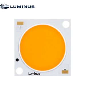
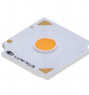
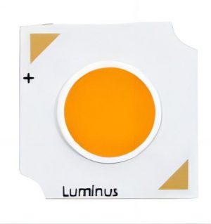
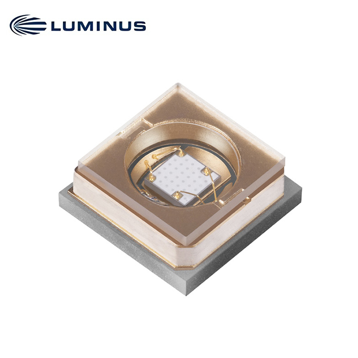
SBT-10X-UV Surface Mount LED
Features
• High power UV LED with peak wavelengths 365 – 425 nm
• Latest UVX technology enables ultra-high power density-operation up to 4 A
• Up to 2 W output to maximize performance of curing systems
• Industry standard 3 5 mm x 3 5 mm package
• 120° viewing angle
• Environmentally friendly: REACH, RoHS and Halogen compliant
Applications
• Curing- inks, coating and adhesives
• 3D Printing
• Maskless Lithography
• Diagnostics
• Fluorescence Imaging
Ordering Part Numbers
| Wavelength Range (nm) | Radiometric Flux | Wavelength Bins | Ordering Part Number1,2 | |
| Bin Kit Code | Min. Flux (W) | |||
| 365-375 | AH | 1 .3 | 365, 370 | SBT-10X-UV-A120-AH365-22 |
| 380-390 | AH | 1 .3 | 380, 385 | SBT-10X-UV-A120-AH380-22 |
| 390-400 | AH | 1 .3 | 390, 395 | SBT-10X-UV-A120-AH390-22 |
| 400-410 | AH | 1 .3 | 400, 405 | SBT-10X-UV-A120-AH400-22 |
| 415-425 | AH | 1 .3 | 415, 420 | SBT-10X-UV-A120-AH415-22 |
Binning Structure
SBT-10X-UV LEDs are specified for radiometric flux and peak wavelength at a drive current of 1.0 A with a 20 ms pulse at 25°C and placed into one of the following Flux, Wavelength and Forward Voltage bins.
Radiometric Flux Bins
| Color | Radiometric Flux Bin (FF) | Minimum Flux (W) | Maximum Flux (W) |
| UV | AH | 1.30 | 1.40 |
| AJ | 1.40 | 1.50 | |
| AK | 1.50 | 1.75 | |
| AL | 1.75 | 2.00 |
Peak Wavelength Bins
| Color | Wavelength Bin (WWW) | Minimum Wavelength (nm) | Maximum Wavelength (nm) |
| UV | 365 | 365 | 370 |
| 370 | 370 | 375 | |
| 380 | 380 | 385 | |
| 385 | 385 | 390 | |
| 390 | 405 | 410 | |
| 395 | 395 | 400 | |
| 400 | 400 | 405 | |
| 405 | 405 | 410 | |
| 415 | 415 | 420 | |
| 420 | 420 | 425 |
Binning Structure
Forward Voltage Bins
| Color | Forward Voltage Bin | Minimum Voltage (V) | Maximum Voltage (V) |
| UV | V0 | 3.0 | 3.1 |
| V1 | 3.1 | 3.2 | |
| V2 | 3.2 | 3.3 | |
| V3 | 3.3 | 3.4 | |
| V4 | 3.4 | 3.5 | |
| V5 | 3.5 | 3.6 | |
| V6 | 3.6 | 3.7 | |
| V7 | 3.7 | 3.8 | |
| V8 | 3.8 | 3.9 | |
| V9 | 3.9 | 4.0 | |
| V10 | 4.0 | 4.1 | |
| V11 | 4.1 | 4.2 |
Typical Device Performance (Tc = 25°C)
| Characteristics at Recommended Test Drive Current | Symbol | 365 nm | 385 nm | 395 nm | 405 nm | 420 nm | Unit | |
| Peak Wavelength Range | typ | λ | 365-375 | 380-390 | 390-400 | 400-410 | 415-425 | nm |
| Test Current 1 | typ | I | 1.0 | 1.0 | 1.0 | 1.0 | 1.0 | A |
| Peak Wavelength Typ. | typ | λp | 367 | 385 | 395 | 405 | 420 | nm |
| Forward Voltage | min | VF min | 3.0 | 3.0 | 3.0 | 3.0 | 3.0 | V |
| typ | VF | 3.7 | 3.4 | 3.6 | 3.7 | 3.7 | V | |
| max | VF max | 4.2 | 4.1 | 4.1 | 4.2 | 4.2 | V | |
| Radiometric Flux 2 | typ | Φtyp | 1.6 | 1.6 | 1.5 | 1.4 | 1.4 | W |
| FWHM at 50% of Φ | typ | Δλ1/2 | 15 | 15 | 15 | 17 | 17 | nm |
| Device Thermal Characteristics at 3 | .0 A 3 | |||||||
| Electrical thermal resistance (junction to case) | typ | Rθj-c (elec.) | 1.8 | °C/W | ||||
| Real thermal resistance
(junction to case) WPE = 31.7% |
typ | Rθj-c (real) | 2.6 | °C/W |
Absolute Maximum Ratings
| Symbol | Values | Unit | |
| Absolute Minimum Current (CW or Pulsed) 1 | Imin | 0.2 | A |
| Absolute Maximum Current for 365 nm (CW) 2 | Imax | 2.5 | A |
| Absolute Maximum Current for 385/395/405/420 nm (CW) 2 | Imax | 4.0 | A |
| Absolute Maximum Surge Current for 365 nm 2 (Frequency > 240 Hz, duty cycle =10%, t=1ms) | Is | 3.75 | A |
| Absolute Maximum Surge Current for 385/395/405/
420 nm 2 (Frequency > 240 Hz, duty cycle =10%, t=1ms) |
Is | 6.0 | A |
| Maximum Junction Temperature 2 | Tjmax | 125 | °C |
| Storage Temperature Range | Ts | -40 to +100 | °C |
| ESD Sensitivity (HBM) | Vb | 8 | kV |