Description
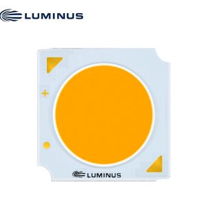
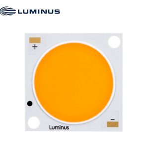
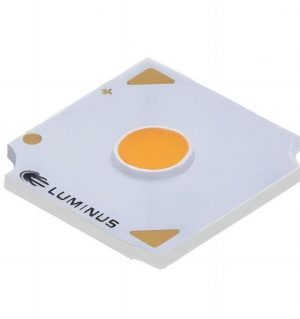
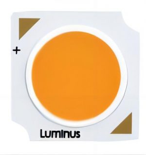
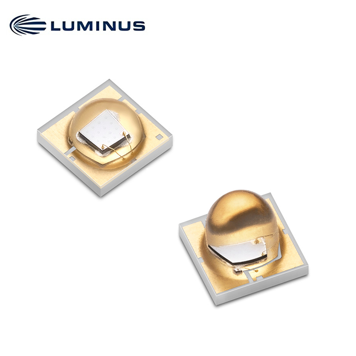
SST-08-UV Surface Mount UVA LED
Features
• High Power UV-A LED series with peak wavelength options of 365 nm, 385 nm, 395 nm and 405 nm
• Sulfur and corrosion resistant package for demanding applications
• Industry standard 3.5 mm x 3.5 mm package
• Drive current up to 750 mA
• Available in 130° and 40° viewing angle
• Built-in ESD Protection
• Environmentally friendly: REACH, RoHS and Halogen compliant
Applications
• Horticulture
• Curing inks, coating and adhesives
• Photocatalytic air/water purification
• Medical and Analytic instrumentation
• Diagnostic
• Fluorescence Imaging
Ordering Part Numbers
| Wavelength
Range |
Wavelength
Bins |
Radiometric Flux | Solder Pad | Viewing Angle | Ordering Part Number | |
| Min. Flux Bin | Min. Flux (mW) | |||||
| 365-375 | 365, 370 | D | 630 | A | 40° | SST-08-UV-A40-D365-00 |
| D | 630 | A | 130° | SST-08-UV-A130-D365-00 | ||
| 380-390 | 380, 385 | E | 720 | A | 40° | SST-08-UV-A40-E385-00 |
| F | 810 | A | 130° | SST-08-UV-A130-F385-00 | ||
| 390-400 | 390, 395 | E | 720 | A | 40° | SST-08-UV-A40-E395-00 |
| F | 810 | A | 130° | SST-08-UV-A130-F395-00 | ||
| 400-410 | 400, 405 | E | 720 | A | 40° | SST-08-UV-A40-E405-00 |
| F | 810 | A | 130° | SST-08-UV-A130-F405-00 | ||
Binning Structure
SST-08-UV LEDs are tested for radiometric flux and wavelength at a drive current of 500 mA, 20 ms single pulse at 25° C and placed into one of the following radiometric flux (F) , wavelength (WWW) and forward voltage bins. The LEDs can also be driven at other drive
currents, to achieve the correlated flux values listed in the table.
Radiometric Flux Bins
| Flux Bin (F)1 | Minimum Flux 3
(mW) 500 mA, 25° C |
Maximum Flux 3
(mW) 500 mA, 25° C |
Correlated Minimum Flux 2
(mW) at 25° C |
||
| 250 mA | 350 mA | 700 mA | |||
| D | 630 | 720 | 315 | 440 | 875 |
| E | 720 | 810 | 360 | 500 | 1000 |
| F | 810 | 900 | 400 | 570 | 1125 |
| G | 900 | 990 | 450 | 630 | 1250 |
| H | 990 | 1080 | 495 | 700 | 1375 |
Wavelength Bins
| Wavelength Bin (WWW) | Minimum Wavelength (nm)3 | Maximum Wavelength (nm)3 |
| 365 | 365 | 370 |
| 370 | 370 | 375 |
| 380 | 380 | 385 |
| 385 | 385 | 390 |
| 390 | 390 | 395 |
| 395 | 395 | 400 |
| 400 | 400 | 405 |
| 405 | 405 | 410 |
Forward Voltage Bins
| Voltage Bin1 | Minimum Voltage (V) | Maximum Voltage (V) |
| V1 | 3.0 | 3.2 |
| V2 | 3.2 | 3.4 |
| V3 | 3.4 | 3.6 |
| V4 | 3.6 | 3.8 |
| V5 | 3.8 | 4.0 |
Typical Device Performance
| Parameter | Symbol | Typical1 | Unit | |||
| Peak Wavelength Range | λ | 365-375 | 380-390 | 390-400 | 400-410 | nm |
| Test Current2 | If | 500 | 500 | 500 | 500 | mA |
| Forward Voltage | Vf-min | 3.0 | 3.0 | 3.0 | 3.0 | V |
| Vf-typ | 3.8 | 3.6 | 3.6 | 3.7 | V | |
| Vf-max | 4.1 | 4.0 | 4.0 | 4.0 | V | |
| Radiometric Flux3 | Φtyp | 690 | 900 | 870 | 850 | mW |
| FWHM | Δλ | 10 | 10 | 10 | 10 | nm |
| Viewing Angle | 2θ1/2 | 40 / 130 | 40 / 130 | 40 / 130 | 40 / 130 | ° |
| Thermal Resistance (junction-solder point) | Rth elec. | 5.0 | 5.0 | 5.0 | 5.0 | °C/W |
Absolute Maximum Ratings
| Parameter | Symbol | Value | Unit |
| Forward Current1 | If-max | 750 | mA |
| Junction Temperature1 | Tj | 100 | ° C |
| Storage Temperature Range | TS | -40 to +100 | ° C |
| Soldering Temperature | TSLD | JEDEC J-STD-020C, 245°C | ° C |