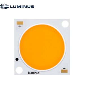
Description
CBT-90-UV High Brightness UV LED
Features
• UV LED with a monolithic chip of emitting area 9 mm2
• Unencapsulated die with low profile protective window optimizes optical coupling in fiber coupling and in etendue-limited applications
• Typical peak emission of 405 nm and 415 nm
• Ultra High thermal conductivity common anode package allows operation at up to 27A
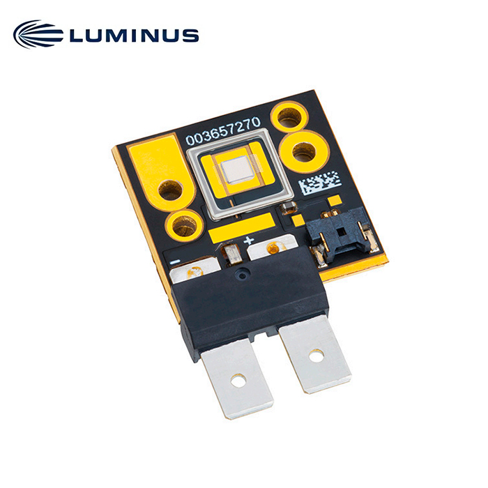
• Chip on board package for easy thermal management and optical integration
• Environmentally friendly: RoHS, REACH and Halogen compliant
CBT-90-UV Binning Structure
CBT-90 UV LEDs are tested at 18 A continuous current, at a constant heat sink temperature of 40°C and placed into one of the following flux and wavelength bins.
Flux Bins*
| Color | Radiometric Flux Bin (F) | Min Radiometric
Power (Watts) @ 18A |
Max Radiometric
Power (Watts) @ 18A |
| UV | P | 16.1 | 17.7 |
| Q | 17.7 | 19.5 | |
| R | 19.5 | 21.4 |
Wavelength Bins
| Color | Peak Wavelength Bin | Min Peak Wavelength
@ 18A |
Max Peak Wavelength
@ 18A |
| UV (Peak WL) | 400 | 400 | 405 |
| 405 | 405 | 410 | |
| 410 | 410 | 415 | |
| 415 | 415 | 420 |
Ordering Part Numbers
| Wavelength Range | Radiometric Flux | Wavelength Bins | Ordering
Part Number2,,3 |
|
| Bin Kit Flux
Code |
Min. Flux | |||
| 400-410 | P | 16.1 | 400, 405 | CBT-90-UV-L11-P400-22 |
| 410-420 | P | 16.1 | 410, 415 | CBT-90-UV-L11-P410-22 |
Typical Device Performance
| UV | ||||
| Parameter | Symbol | Values 4 | Unit | |
| Peak Wavelength Range | λ | 400-410 | 410-420 | nm |
| Test Current for binning 5 | I | 18.0 | 18.0 | A |
| Peak Wavelength Typ. | λp | 405 | 415 | nm |
| Forward Voltage | VF min | 3.0 | 3.0 | V |
| VF | 3.6 | 3.6 | V | |
| VF max | 4.4 | 4.4 | V | |
| Radiometric Flux 6 | Φtyp | 19.5 | 19.5 | W |
| FWHM at 50% of Φ | Δλ1/2 | 20 | 20 | nm |
| Symbol | Values 4 | Unit | |
| Absolute Minimum Current (CW or Pulsed)7 | 1.0 | A | |
| Absolute Maximum Current (CW)8 | 27 | A | |
| Absolute Maximum Surge Current 8
(Frequency > 240 Hz, duty cycle =10%, t=1ms) |
31.5 | A | |
| Absolute Maximum Junction Temperature 8 | Tjmax | 150 | ºC |
| Storage Temperature Range | -40/+100 | ºC | |
| Emitting Area9 | A e | 9.0 | mm2 |
| Emitting Area Dimensions | 3.0 x 3.0 | mm × mm |