Description
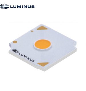
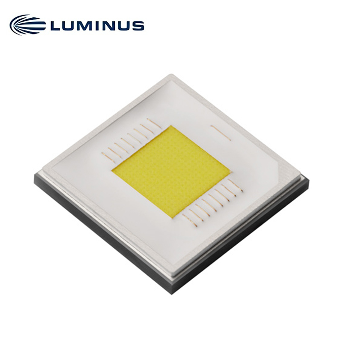
SFT-90X-WS65-M2 High Power White LEDs
Features
SFT white series is a powerful light source for beam pattern critical lighting applications. The flat window of an SFT white LED results in a much smaller light emitting surface than a dome-shaped cover, enabling smaller optics and higher optical efficiency in directional lighting systems.
• Ultra-high flux from a single large chip, with a maximum output of 5500 lm @ 20 A, 85°C.
• Vertical chip with high lumen density and small emitting angle, ideal for efficient optical beam shaping to achieve high intensity, narrow beam angle and long beam distance.
• Phosphor-on-chip with superior color uniformity over radiation angles, delivering homogeneous color in beam spots.
• Maximum Drive Current: 20 A
• Color Temperature: 6500K
• Color Rendering Index: Typ. 70
• Low thermal resistance: 0.35 °C/W
• Electrically isolated thermal path
• 8 kV HBM ESD rating per ANSI/ESDA/JEDEC JS-001
Applications
• Portable Lighting
• Battery or Solar Powered Lights
• LED Work Lights
• Beacons
• Outdoor Lighting
Ordering Part Numbers
| CRI | CCT | Luminous Flux | Chromaticity
Bin Kit3 |
Ordering Part Numbers | |
| Minimum
Flux Bin1 |
Minimum
Flux² |
||||
| Typ. 70
Min. 65 |
6500K | J7 | 3195 lm | 651 | SFT-90X-WS65-M2-J7651 |
| 652 | SFT-90X-WS65-M2-J7652 | ||||
| 653 | SFT-90X-WS65-M2-J7653 | ||||
| J8 | 3400 lm | 651 | SFT-90X-WS65-M2-J8651 | ||
| 652 | SFT-90X-WS65-M2-J8652 | ||||
| 653 | SFT-90X-WS65-M2-J8653 | ||||
Binning Structure
Luminous Flux Bins1,2
| Flux Bin | Binning @ 10.0 A | Correlated Minimum Flux (lm) @ Tj=85°C2 | |||||
| Tj= 85°C1 | Tj= 25°C1 | 2.0 A | 5.0 A | 15.0 A | 20.0 A | ||
| Minimum
Flux (lm) |
Maximum
Flux (lm) |
Minimum
Flux (lm) |
|||||
| J7 | 3195 | 3400 | 3553 | 831 | 1853 | 4313 | 5176 |
| J8 | 3400 | 3635 | 3781 | 884 | 1972 | 4590 | 5508 |
| J9 | 3635 | 3870 | 4042 | 945 | 2108 | 4907 | 5889 |
| K1 | 3870 | 4140 | 4303 | 1006 | 2245 | 5225 | 6269 |
Forward Voltage Bins3
| Voltage Bin | Binning @ 10.0 A, Tj = 85°C | |
| Minimum Voltage (V) | Maximum Voltage (V) | |
| VK | 2.9 | 3.1 |
| VL | 3.1 | 3.3 |
Binning Structure
Chromaticity Binning Coordinates
| CCT | Bin | CIEx | CIEy | Bin | CIEx | CIEy | Bin | CIEx | CIEy | Bin | CIEx | CIEy |
| 6500K | BA | 0.3048 | 0.3207 | BB | 0.3028 | 0.3304 | BC | 0.3115 | 0.3391 | BD | 0.3130 | 0.3290 |
| 0.3130 | 0.3290 | 0.3115 | 0.3391 | 0.3205 | 0.3481 | 0.3213 | 0.3373 | |||||
| 0.3144 | 0.3186 | 0.3130 | 0.3290 | 0.3213 | 0.3373 | 0.3221 | 0.3261 | |||||
| 0.3068 | 0.3113 | 0.3048 | 0.3207 | 0.3130 | 0.3290 | 0.3144 | 0.3186 | |||||
| BH | 0.3068 | 0.3113 | BE | 0.3005 | 0.3415 | BF | 0.3099 | 0.3509 | BG | 0.3144 | 0.3186 | |
| 0.3144 | 0.3186 | 0.3099 | 0.3509 | 0.3196 | 0.3602 | 0.3221 | 0.3261 | |||||
| 0.3161 | 0.3059 | 0.3115 | 0.3391 | 0.3205 | 0.3481 | 0.3231 | 0.3120 | |||||
| 0.3093 | 0.2993 | 0.3028 | 0.3304 | 0.3115 | 0.3391 | 0.3161 | 0.3059 | |||||
| 7500K | AD | 0.2984 | 0.3133 | AG | 0.3037 | 0.2937 | AH | 0.2980 | 0.2880 | |||
| 0.3048 | 0.3207 | 0.3009 | 0.3042 | 0.2950 | 0.2970 | |||||||
| 0.3068 | 0.3113 | 0.3068 | 0.3113 | 0.3009 | 0.3042 | |||||||
| 0.3009 | 0.3042 | 0.3093 | 0.2993 | 0.3037 | 0.2937 |
Absolute Maximum Ratings
| Parameter | Symbol | Value | Unit | |
| DC Forward Current | Minimum | If min | 0.1 | A |
| Maximum | If max | 20 | ||
| Surge Current (t<10 ms, Duty Cycle < 10%) | I
s |
22 | A | |
| Reverse Voltage (Ir= 10 mA) | V r | 5 | V | |
| Power Dissipation | PD | 72 | W | |
| Junction Temperature | Tj max | 150 | °C | |
| Operating Temperature Range | T
opr |
-40 to 100 | °C | |
| Storage Temperature Range | T
stg |
-40 to 100 | °C | |
| ESD withstand Voltage ANSI/ESDA/JEDEC JS-001 (HBM) | VHBM | 8 | kV | |
| ESD withstand Voltage ANSI/ESDA/JEDEC JS-002 (CDM) | VCDM | 1 | kV | |
Characteristics
| Parameter | Symbol | Value | Unit | |
| Color Rendering Index1 (Tj= 85°C) | Minimum | CRI
min |
65 | |
| Typical | CRItyp | 70 | ||
| Forward Voltage (If= 10.0 A, Tj= 85°C) | Minimum | Vf min | 2.9 | V |
| Typical | Vf typ | 3.2 | ||
| Maximum | Vf max | 3.3 | ||
| Viewing Angle (FWHM) | 2θ1/2 | 120 | ° | |
| Temperature Coefficient of Voltage | ∂Vf/∂T | -1.0 | mV/°C | |
| Electrical Thermal Resistance (Junction to Solder Point)2 | Rth JS elec | 0.35 | °C/W | |