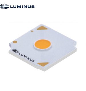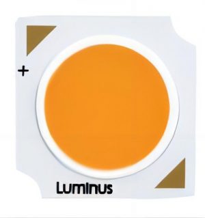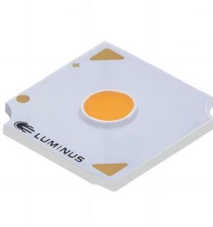
Description
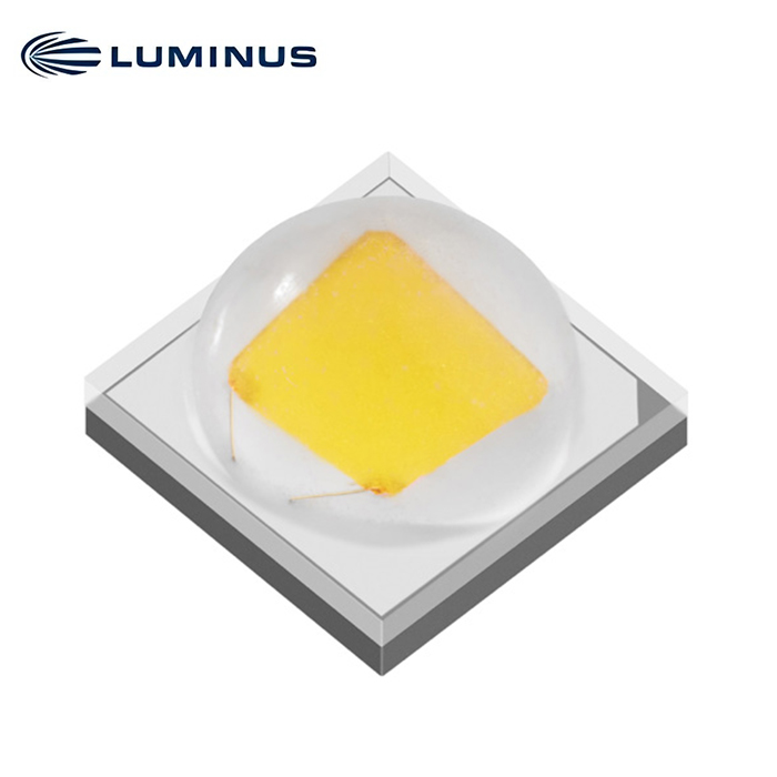
SST-20V-WES (CRI > 70) The V-Line High Power White LEDs
Features
• High CRI, high-efficacy white LEDs for high-performance directional lighting applications.
• The vertical chip features high lumen density and small emitting angle, ideal for maximizing the light intensity and reducing the optics size in optical beam shaping.
• The phosphor-on-chip technology delivers high color uniformity over radiation angle, enabling superior light quality for beam spots.
• Maximum Drive Current: 3.0 A
• Color Temperature: 4000K, 5700K, 6500K
• Color Rendering Index: 65, 70
• Low thermal resistance: 1.6 °C/W
• ANSI-compatible chromaticity bins
• Electrically isolated thermal path
• 8 kV HBM ESD rating per ANSI/ESDA/JEDEC JS-001
Applications
• Landscape Lighting
• Garage and Canopy Lights
• High / Low Bay Industrial Lighting
• Automotive Auxiliary Lights
• Roadway and Street Lighting
• Sports Field Lighting
• Outdoor Area Lighting
• LED Work Lights
• Portable Lights
Ordering Part Numbers
| CRI | CCT | Luminous Flux | Ordering Part Number | ||
| Minimum
Flux Bin1 |
Minimum Flux² | Chromaticity Bin Kit ANSI Centers | Chromaticity Bin Kit 5-Step Ellipse | ||
| Typ. 70, Min. 65 | 6500K | D6 | 340 lm | SST-20V-WS65-A2-D6652 | – |
| > 70 | 4000K | D6 | 340 lm | SST-20V-WE40-A2-D6402 | SST-20V-WE40-A2-D640E5 |
| D7 | 355 lm | SST-20V-WE40-A2-D7402 | SST-20V-WE40-A2-D740E5 | ||
| 5700K | D6 | 340 lm | SST-20V-WE57-A2-D6572 | SST-20V-WE57-A2-D657E5 | |
| D7 | 355 lm | SST-20V-WE57-A2-D7572 | SST-20V-WE57-A2-D757E5 | ||
| 6500K | D5 | 325 lm | SST-20V-WE65-A2-D5652 | SST-20V-WE65-A2-D565E5 | |
| D6 | 340 lm | SST-20V-WE65-A2-D6652 | SST-20V-WE65-A2-D665E5 | ||
Luminous Flux Bins
| Flux Bin | Binning @ 700 mA | Correlated Minimum Flux (lm) @ Tj=85°C2 | ||||||
| T = 85°C
j |
T = 25°C
j |
|||||||
| Minimum
Flux (lm) |
Maximum
Flux (lm) |
Minimum
Flux (lm) |
350 mA | 1000 mA | 1500 mA | 2000 mA | 3000 mA | |
| D5 | 325 | 340 | 358 | 176 | 442 | 618 | 770 | 1030 |
| D6 | 340 | 355 | 374 | 184 | 462 | 646 | 806 | 1078 |
| D7 | 355 | 375 | 391 | 192 | 483 | 675 | 841 | 1125 |
| D8 | 375 | 395 | 413 | 203 | 510 | 713 | 889 | 1189 |
Forward Voltage Bins
| Voltage Bin | Binning @ 700 mA, Tj= 85°C | |
| Minimum Voltage (V) | Maximum Voltage (V) | |
| VH | 2.5 | 2.7 |
| VJ | 2.7 | 2.9 |
| VK | 2.9 | 3.1 |
Binning Structure
Chromaticity Binning Coordinates (ANSI Centers)
| CCT | Bin | CIEx | CIEy | Bin | CIEx | CIEy | Bin | CIEx | CIEy | Bin | CIEx | CIEy |
| 4000K | FA3 | 0.3744 | 0.3685 | FB4 | 0.3763 | 0.3760 | FC1 | 0.3825 | 0.3798 | FD2 | 0.3804 | 0.3721 |
| 0.3763 | 0.3760 | 0.3782 | 0.3837 | 0.3847 | 0.3877 | 0.3825 | 0.3798 | |||||
| 0.3825 | 0.3798 | 0.3847 | 0.3877 | 0.3912 | 0.3917 | 0.3887 | 0.3836 | |||||
| 0.3804 | 0.3721 | 0.3825 | 0.3798 | 0.3887 | 0.3836 | 0.3863 | 0.3758 | |||||
| 5700K | CA | 0.3215 | 0.3350 | CB | 0.3207 | 0.3462 | CC | 0.3290 | 0.3538 | CD | 0.3290 | 0.3417 |
| 0.3290 | 0.3417 | 0.3290 | 0.3538 | 0.3376 | 0.3616 | 0.3371 | 0.3490 | |||||
| 0.3290 | 0.3300 | 0.3290 | 0.3417 | 0.3371 | 0.3490 | 0.3366 | 0.3369 | |||||
| 0.3222 | 0.3243 | 0.3215 | 0.3350 | 0.3290 | 0.3417 | 0.3290 | 0.3300 | |||||
| 6500K | BA | 0.3048 | 0.3207 | BB | 0.3028 | 0.3304 | BC | 0.3115 | 0.3391 | BD | 0.3130 | 0.3290 |
| 0.3130 | 0.3290 | 0.3115 | 0.3391 | 0.3205 | 0.3481 | 0.3213 | 0.3373 | |||||
| 0.3144 | 0.3186 | 0.3130 | 0.3290 | 0.3213 | 0.3373 | 0.3221 | 0.3261 | |||||
| 0.3068 | 0.3113 | 0.3048 | 0.3207 | 0.3130 | 0.3290 | 0.3144 | 0.3186 |
Absolute Maximum Ratings
| Parameter | Symbol | Values | Unit | ||
| T =130°C
j |
T =150°C
j |
||||
| Forward Current | Minimum | If min | 0.1 | A | |
| Maximum | If max | 3.0 | 2.0 | ||
| Surge Current (t<10 ms, Duty Cycle < 10%) | I
s |
4.0 | 3.0 | ||
| Power Dissipation | PD | 11 | 7 | W | |
| Reverse Voltage (@ If= 10 mA) | V r | 5 | V | ||
| Junction Temperature | T
j |
150 | °C | ||
| Operating Temperature Range | T
opr |
-40 to 100 | |||
| Storage Temperature Range | T
stg |
-40 to 100 | |||
| ESD withstand Voltage ANSI/ESDA/JEDEC JS-001 (HBM) | VESD | 8 | kV | ||
| ESD withstand Voltage ANSI/ESDA/JEDEC JS-002 (CDM) | VCDM | 1 | |||
Characteristics
| Parameter (If=700 mA, Tj=85°C) | Symbol | Value | Unit | ||
| WS | WE | ||||
| Color Rendering Index1 | CRImin | > 65 | > 70 | ||
| Forward Voltage | Minimum | Vf min | 2.5 | V | |
| Typical | Vf typ | 2.9 | |||
| Maximum | Vf max | 3.1 | |||
| Viewing Angle | 2θ1/2 | 118 | ° | ||
| Temperature Coefficient of Voltage | ∂Vf/∂T | -1.2 | mV/°C | ||
| Electrical Thermal Resistance (Junction to Solder Point)2 | Rth JS elec | 1.6 | °C/W | ||