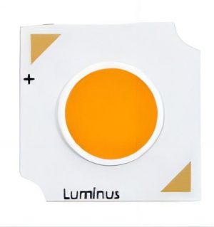
Description
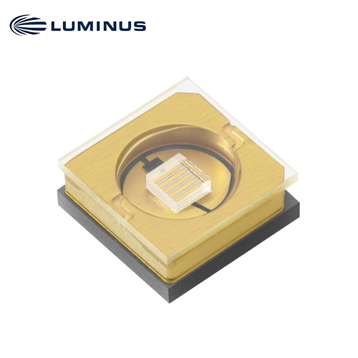
XBT-3535-265/275 nm Surface Mount UVC LED
Features
• UV LED with peak wavelengths 265 nm and 275 nm
• High Optical Power: Up to 135 mW of UVC power at maximum rated current
• Compact form factor: 3.5 mm x 3.5 mm package with optically transparent window
• Viewing angle of 130 degrees
• Standard SMT process
Applications
• Water/ Air/ Surface Disinfection
• Healthcare
• Food & Pharmaceutical Processing
• Analytical Instruments
• Horticulture
Ordering Part Numbers1
| Wavelength Range
(nm) |
Wavelength Bins | Radiometric Flux | Ordering Part Number | |
| Bin Kit Flux Code | Min. Flux (mW) | |||
| 260 – 270 | 260, 265 | CH | 55 | XBT-3535-UV-A130H-CH260-00 |
| 270 – 280 | 270, 275 | DA | 60 | XBT-3535-UV-A130H-DA270-00 |
Binning Structure
XBT-3535-UV LEDs are tested at a drive current of 500 mA, 20 ms single pulse at 25°C and placed into one of the following radiometric flux and wavelength bins. The LEDs can also be driven at different drive currents to achieve the correlated flux values listed in the table.
Radiometric Flux Bins1,2
| Color | Flux Bin3 | Binning @ 500 mA, Tc= 25°C4,5 | Correlated Minimum Flux (mW) @ Tc= 25°C | |||
| Min. Flux (mW) | Max. Flux (mW) | 350 mA | 650 mA | 800 mA | ||
| uv | CH | 55 | 60 | 41 | 68 | 81 |
| DA | 60 | 70 | 44 | 75 | 89 | |
| DB | 70 | 80 | 52 | 87 | 103 | |
| DC | 80 | 90 | 59 | 100 | 118 | |
| DD | 90 | 100 | 66 | 112 | 133 | |
| DE | 100 | 120 | 74 | 125 | 148 | |
| FA | 120 | 140 | 88 | 149 | 177 | |
Binning Structure
XBT-3535-UV LEDs are tested at a drive current of 500 mA, 20 ms single pulse at 25°C and placed into one of the following radiometric flux and wavelength bins. The LEDs can also be driven at different drive currents to achieve the correlated flux values listed in the table.
Wavelength Bins2
| Color | Wavelength Bin3,6 | Binning @ 500 mA, Tc= 25°C4,5 | |
| Minimum Wavelength (nm) | Maximum Wavelength (nm) | ||
| uv | 260 | 260 | 265 |
| 265 | 265 | 270 | |
| 270 | 270 | 275 | |
| 275 | 275 | 280 | |
Forward Voltage Bins
| Color | Voltage Bin | Binning @ 500 mA, Tc= 25°C | |
| Minimum Voltage (V) | Maximum Voltage (V) | ||
| uv | V3 | 5 | 5.5 |
| V4 | 5.5 | 6 | |
| V5 | 6 | 6.5 | |
| V6 | 6.5 | 7 | |
| V7 | 7 | 7.5 | |
Absolute Maximum Ratings1
| Parameter | Symbol | Value | Unit |
| Forward Current | If max | 800 | mA |
| Storage Temperature | T
s min |
-40 | °C |
| T
s max |
100 | ||
| Junction Temperature | Tj max | 100 | °C |
| ESD sensitivity
ANSI/ESDA/JEDEC JS-001 (HBM, Class 3B) |
VESD | 8000 | V |
Device Performance1,2
| Optical and Electrical Characteristics | Symbol | Value | Unit |
| Test Current | If | 500 | mA |
| Forward Voltage | Vf min | 5.0 | V |
| Vf typ | 5.9 | ||
| Vf max | 7.5 | ||
| FWHM | ∆λ | 13 | nm |
| Viewing Angle | 2θ1/2 | 130 | ° |
| Thermal Characteristics | |||
| Thermal Resistance (junction to case)3 | RѲj-c | 5.4 | °C/W |