Description
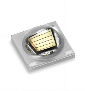
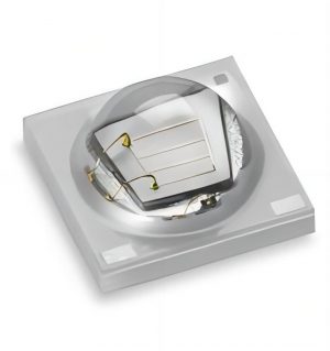
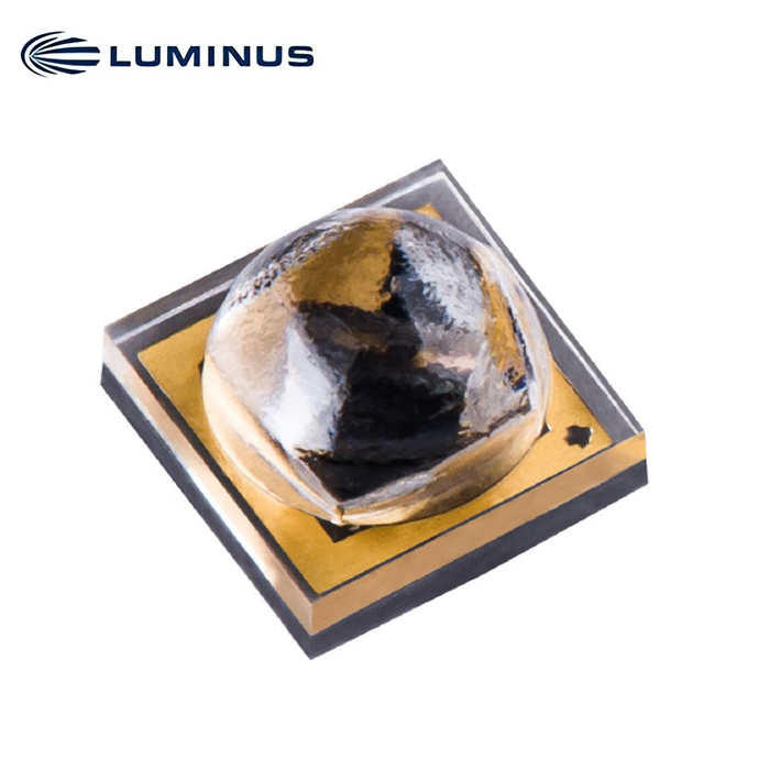
XST-3535-UV Surface Mount UVC LED
Features
• UVC LED with emission wavelength between 270 nm and 285 nm
• High Optical Power: 100 mW+ of UVC power at maximum rated current
• Compact form factor: 3.5 mm x 3.5 mm package
• Narrow viewing angle of 60 degrees
• Standard SMT Process
• RoHS and REACH compliant
Applications
• Air Purification
• Water Purification
• Surface Disinfection
• Medical Device Sterilization
• Appliance Sterilization
• Food & Beverage Preparation
Ordering Part Numbers
The table below lists ordering part numbers available for XST-3535-UV LEDs. The part number includes a bin kit, a group of flux and wavelength bins described in page 3, that are shippable for a given ordering part number. Individual flux bins are not orderable. Flux bin listed is minimum bin shipped – higher bins may be included at Luminus’discretion.
| Wavelength | Radiometric Flux | Ordering Part Number | ||
| Range (nm) | Bin kit | Bin Kit Flux Code | Min. Flux (mW) | |
| 270-280 | 270, 275 | CD | 35 | XST-3535-UV-A60-CD270-00 |
| 275-280 | 275 | CD | 35 | XST-3535-UV-A60-CD275-01 |
| 275-285 | 275, 280 | CD | 35 | XST-3535-UV-A60-CD275-00 |
| 270-280 | 270, 275 | CE | 40 | XST-3535-UV-A60-CE270-00 |
| 275-280 | 275 | CE | 40 | XST-3535-UV-A60-CE275-01 |
| 275-285 | 275, 280 | CE | 40 | XST-3535-UV-A60-CE275-00 |
XST-3535-UV Binning Structure
XST-3535-UV LEDs are tested at a drive current of 350 mA, 20 ms single pulse at 25 °Cand placed into one of the following radiometric flux (FF), wavelength (WWW) and forward voltage bins.
Radiometric Flux Bins1
The LEDs can also be driven at higher drive currents, to achieve the correlated flux values listed in the table.
| Flux Bin | Binning @ 350 mA, 25 °C | Correlated Minimum Flux (mW) @ 25 °C | |||
| Mini Flux (mW) | Max Flux (mW) | 500 mA | 650 mA | 800 mA | |
| CD | 35 | 40 | 49 | 64 | 79 |
| CE | 40 | 45 | 56 | 74 | 90 |
| CF | 45 | 50 | 63 | 83 | 101 |
| CG | 50 | 55 | 70 | 92 | 113 |
| CH | 55 | 60 | 77 | 101 | 124 |
| DA | 60 | 70 | 84 | 110 | 135 |
Wavelength Bins2,3
| Wavelength Bin | Binning @ 350 mA, 25 °C | |
| Minimum Wavelength (nm) | Maximum Wavelength (nm) | |
| 270 | 270 | 275 |
| 275 | 275 | 280 |
| 280 | 280 | 285 |
Forward Voltage Bins
| Voltage Bin | Binning @ 350 mA, 25 °C | |
| Minimum Forward Voltage (V) | Maximum Forward Voltage (V) | |
| V3 | 5.0 | 5.5 |
| V4 | 5.5 | 6.0 |
| V5 | 6.0 | 6.5 |
| V6 | 6.5 | 7.0 |
| V7 | 7.0 | 7.5 |
Typical Device Performance1,2
| Parameter | Symbol | Value | Unit |
| Minimum Forward Voltage | Vf-min | 5.0 | V |
| Typical Forward Voltage | Vf-typ | 6.45 | V |
| Maximum Forward Voltage | Vf-max | 7.5 | V |
| FWHM | Δλ | 10 | nm |
| Viewing Angle | 2θ1/2 | 60 | ° |
| Thermal Resistance (junction-solder point) | Rth | 5.0 | °C/W |
Absolute Maximum Ratings2
| Parameter | Symbol | Value | Unit |
| Forward Current | If-max | 800 | mA |
| Junction Temperature | Tj | 100 | °C |