Description
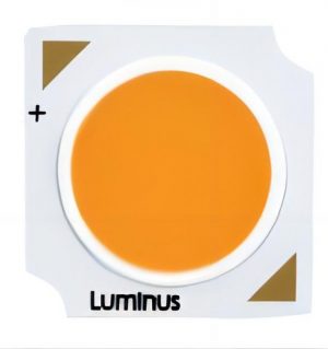
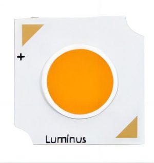
SFT-25R-WG (CRI > 90) High Power White LEDs
Features
With Luminus’ advanced chip and packaging technologies, SFT-25R-W maximizes the Candela/Lumen K-Factor for high optical performance in directional lighting:
• A small emitter enables high intensity, long beam distance and small optics.
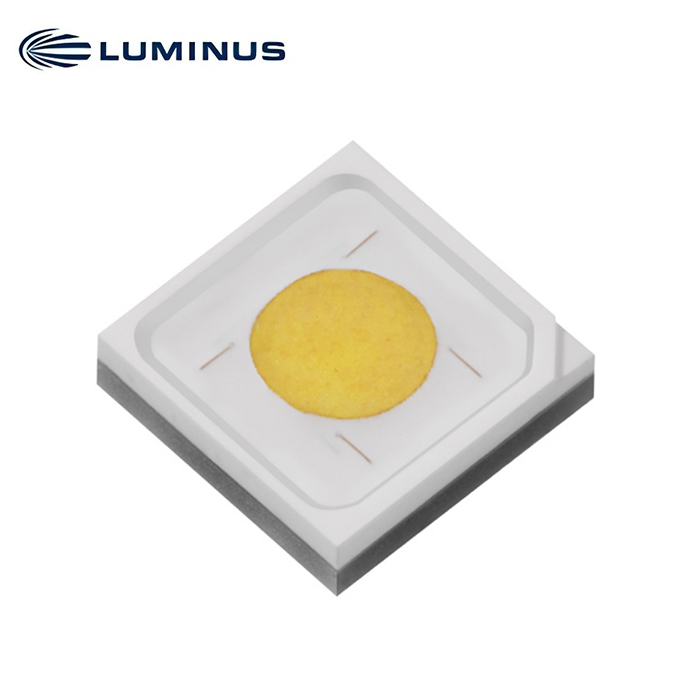
• A patented round emitter, in comparison with a square emitter, enables better uniformity and higher intensity in beam spots.
• A flat window, in comparison with a domed cover, allows the optics to be closer to the emitter to achieve higher intensity and longer beam distance. In addition, Luminus phosphor-on-chip technology’s high uniformity of color over radiation angle enables superior beam spot light quality.
• Package Size: 3535
• Maximum Drive Current: 5 A
• Color Temperature: 5700K
• Color Rendering Index: > 90
• Low thermal resistance: 0.8 °C/W
• ANSI-compatible chromaticity bins
• Electrically isolated thermal path
• 8 kV HBM ESD rating per ANSI/ESDA/JEDEC JS-001
Applications
• Landscape Lighting
• Garage and Canopy Lights
• High / Low Bay Industrial Lighting
• Stage and Studio Lighting
• Stadium and Sports Field Lighting
• Roadway and Outdoor Lighting
• Track Light
• Spotlight
• Wall Washer
• Task Light
Ordering Part Numbers1
| CRI | CCT | Luminous Flux | Ordering Part Number | |||
| Minimum
Flux Bin1 |
Minimum
Flux² |
|||||
| Chromaticity Bin Kit ANSI Centers | Chromaticity Bin Kit 3-Step Ellipse | Chromaticity Bin Kit 5-Step Ellipse | ||||
| > 90 | 5700K | F2 | 440 lm | SFT-25R-WG57-AV2-F2572 | SFT-25R-WG57-AV2-F257E3 | SFT-25R-WG57-AV2-F257E5 |
| F3 | 465 lm | SFT-25R-WG57-AV2-F3572 | SFT-25R-WG57-AV2-F357E3 | SFT-25R-WG57-AV2-F357E5 | ||
Binning Structure
Luminous Flux Bins1,2
| Flux Bin | Binning @ 1500 mA | Correlated Minimum Flux (lm) @ Tj=85°C2 | |||||
| T = 85°C
j |
T = 25°C
j |
||||||
| Minimum
Flux (lm) |
Maximum
Flux (lm) |
Minimum
Flux (lm) |
1000 mA | 3000 A | 4000 A | 5000 mA | |
| F1 | 415 | 440 | 465 | 295 | 718 | 884 | 1021 |
| F2 | 440 | 465 | 493 | 312 | 761 | 937 | 1082 |
| F3 | 465 | 490 | 521 | 330 | 804 | 990 | 1144 |
| F4 | 490 | 520 | 549 | 348 | 848 | 1044 | 1205 |
Forward Voltage Bins3
| Voltage Bin | Binning @ 1500 mA, Tj= 85°C | |
| Minimum Voltage (V) | Maximum Voltage (V) | |
| VJ | 2.7 | 2.9 |
| VK | 2.9 | 3.1 |
| VL | 3.1 | 3.3 |
Binning Structure
Chromaticity Binning Coordinates (ANSI Centers)
| CCT | Bin | CIEx | CIEy | Bin | CIEx | CIEy | Bin | CIEx | CIEy | Bin | CIEx | CIEy |
| 5700K | CA | 0.3215 | 0.3350 | CB | 0.3207 | 0.3462 | CC | 0.3290 | 0.3538 | CD | 0.3290 | 0.3417 |
| 0.3290 | 0.3417 | 0.3290 | 0.3538 | 0.3376 | 0.3616 | 0.3371 | 0.3490 | |||||
| 0.3290 | 0.3300 | 0.3290 | 0.3417 | 0.3371 | 0.3490 | 0.3366 | 0.3369 | |||||
| 0.3222 | 0.3243 | 0.3215 | 0.3350 | 0.3290 | 0.3417 | 0.3290 | 0.3300 |
Chromaticity Binning Coordinates (3-Step & 5-Step Ellipse)
| CCT | Center Point | 3-Step Ellipse | 5-Step Ellipse | Angle | |||
| CIEx | CIEy | a | b | a | b | ||
| 5700K | 0.3287 | 0.3417 | 0.0072 | 0.0032 | 0.0119 | 0.0052 | 59.09° |
Absolute Maximum Ratings
| Parameter | Symbol | Values | Unit | |
| Forward Current | Minimum | If min | 0.1 | A |
| Maximum | If max | 5.0 | ||
| Surge Current (t<10 ms, Duty Cycle < 10%) | I
s |
6.0 | ||
| Power Dissipation | PD | 18 | W | |
| Reverse Voltage (@ If= 10 mA) | V r | 5 | V | |
| Junction Temperature | T
j |
150 | °C | |
| Operating Temperature Range | T
opr |
-40 to 100 | ||
| Storage Temperature Range | T
stg |
-40 to 100 | ||
| ESD withstand Voltage ANSI/ESDA/JEDEC JS-001 (HBM) | VESD | 8 | kV | |
| ESD withstand Voltage ANSI/ESDA/JEDEC JS-002 (CDM) | VCDM | 1 | ||
Characteristics
| Parameter (If=1500 mA, Tj=85°C) | Symbol | Value | Unit | |
| Color Rendering Index1 | CRI | > 90 | ||
| Forward Voltage | Minimum | Vf min | 2.7 | V |
| Typical | Vf typ | 2.9 | ||
| Maximum | Vf max | 3.3 | ||
| Viewing Angle | 2θ1/2 | 115 | ° | |
| Temperature Coefficient of Voltage | ∂Vf/∂T | -1.4 | mV/°C | |
| Electrical Thermal Resistance (Junction to Solder Point)2 | Rth JS elec | 0.8 | °C/W | |