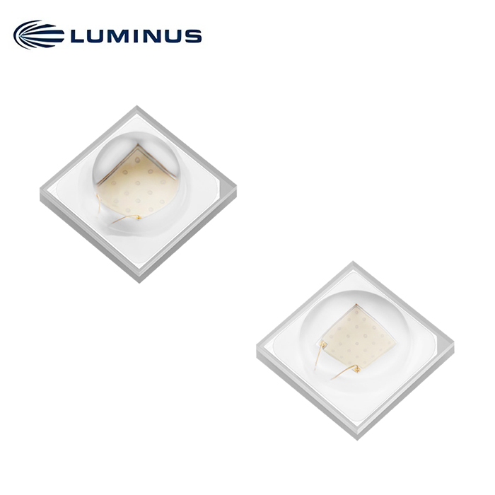
Description
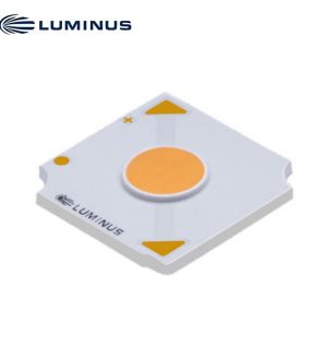
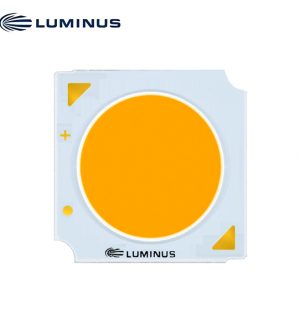
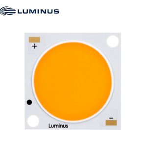
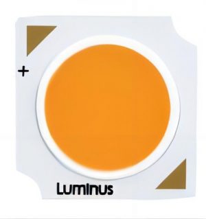
SST-10-G Green LED
Features
• High Power Green LED with typical Peak Wavelength of 527 nm
• Wall-Plug Efficiency: typ. 34% @350 mA
• 90 or 130° viewing angle at 50% Iv
• Low Thermal Resistance
• 6 kV HBM ESD rating per ANSI/ESDA/JEDEC JS-001
Applications
• Industrial / Machine Vision
• Life sciences / Medical
• Accent and effect lighting
• Architectural lighting
• Stage lighting
Ordering Part Numbers
| Color | Radiometric Flux | Wavelength Bin | Viewing Angle | Ordering Part
Number |
|
| Minimum Flux Bin1 | Minimum Flux² | ||||
| Green | F | 230 mW | G3, G4, G5, G6, G7 | 130° | SST-10-G-B130-F530 |
| 90° | SST-10-G-B90-F530 | ||||
Part Number Nomenclature
SST 10 G <B###> <ffwww>
| Product Family | Chip Area | Color | Package Configuration | Bin Kit |
| S: Surface Mount
S: Dome Lensed T: Single Emitter |
10: 1.0 mm2 | G: Green | <B> Solder Pad Configuration
B: type B – see page 13 & 14 <###> Viewing Angle 130: 130° 90: 90° |
<ff> Minimum Flux Bin
<www> Wavelength BinKit See ‘Binning Structure’ on page 3 for details |
Binning Structure
Radiometric Flux Bins1
| Flux Bin | Binning @ 350 mA, Tj= 25°C | |
| Minimum Flux (mW) | Maximum Flux (mW) | |
| F | 230 | 270 |
| G | 270 | 310 |
| H | 310 | 350 |
| J | 350 | 390 |
Forward Voltage Bins2
| Voltage Bin | Binning @ 350 mA, Tj= 25°C | |
| Minimum Voltage (V) | Maximum Voltage (V) | |
| V1 | 2.4 | 2.9 |
Peak Wavelength Bins
| Wavelength Bin | Binning @ 350 mA, Tj= 25°C | |
| Minimum Wavelength (nm) | Maximum Wavelength (nm) | |
| G3 | 515 | 520 |
| G4 | 520 | 525 |
| G5 | 525 | 530 |
| G6 | 530 | 535 |
| G7 | 535 | 540 |
Binning Structure
Radiometric Power to Lumens Conversion1
| Radiometric Power to Lumens | Peak Wavelength (nm) | ||||||
| > 515 nm | > 520 nm | > 525 nm | > 530 nm | > 535 nm | |||
| Flux Bin | F | > 230 mW | 98 – 126 lm | 108 – 137 lm | 117 – 146 lm | 124 – 154 lm | 131 – 160 lm |
| G | > 270 mW | 115 – 145 lm | 126 -157 lm | 137 -168 lm | 146 – 177 lm | 154 -183 lm | |
| H | > 310 mW | 132 – 164 lm | 145 – 177 lm | 157 – 189 lm | 168 – 199 lm | 177 – 207 lm | |
| J | > 350 mW | 149 – 182 lm | 164 – 198 lm | 177 – 211 lm | 189 – 222 lm | 199 – 231 lm | |
Characteristics
| Parameter (If= 350 mA, Tj= 25°C) | Symbol | Value | Unit | |
| Forward Voltage | Minimum | Vf min | 2.4 | V |
| Typical | Vf typ | 2.6 | ||
| Maximum | Vf max | 2.9 | ||
| Forward Current | If | 350 | mA | |
| Typical Radiometric Flux | Φr | 310 | mW | |
| Wall Plug Efficiency | WPE | 34 | % | |
| FWHM | Minimum | 1/2 min | 30 | nm |
| Typical | Δλ
1/2 typ |
33 | ||
| Maximum | 1/2 max | 36 | ||
| Viewing Angle | 2θ1/2 | 90 or 130 | ° | |
| Peak Wavelength | Minimum | λp min | 515 | nm |
| Typical | λp typ | 527 | ||
| Maximum | λp max | 540 | ||
| Electrical Thermal Resistance (Junction to Solder Point)1 | Rth JS elec | 5.3 | °C/W | |
Absolute Maximum Ratings1, 2
| Parameter | Symbol | Values | Unit | |
| Forward Current (CW) | Minimum | If CW min | 0.1 | A |
| Maximum | If CW max | 1.5 | ||
| Reverse Voltage | V r | 5 | V | |
| Power Dissipation | PD | 5 | W | |
| Junction Temperature | T
j |
115 | °C | |
| Storage Temperature Range | T
stg |
-40 to 100 | °C | |
| ESD withstand Voltage ANSI/ESDA/JEDEC JS-001 (HBM, Class) | VESD | 6 | kV | |